- Home
- About us
- EDITORIAL BOARD
- INSTRUCTION TO AUTHOR
- Current Issue
- Archive
- November, 2025
- October, 2025
- September, 2025
- August, 2025
- July, 2025
- June, 2025
- May, 2025
- April, 2025
- March, 2025
- February, 2025
- January, 2025
- December, 2024
- November, 2024
- Ocotber, 2024
- September, 2024
- August, 2024
- July 2024
- June 2024
- May 2024
- April 2024
- March 2024
- February 2024
- January 2024
- December 2023
- November, 2023
- October 2023
- September 2023
- August 2023
- July 2023
- June 2023
- May 2023
- April 2023
- March 2023
- February 2023
- January 2023
- December 2022
- November 2022
- October 2022
- September 2022
- August 2022
- July 2022
- June 2022
- May 2022
- April 2022
- March 2022
- February 2022
- January 2022
- December 2021
- November, 2021
- October, 2021
- September, 2021
- August, 2021
- July, 2021
- June, 2021
- May, 2021
- April 2021
- March 2021
- February 2021
- January 2021
- Submit Article
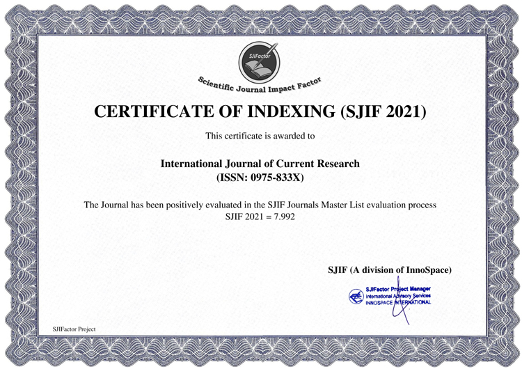
- Certificate
- Reviewers Form
- Contact Us


